
Abstract
We have characterized the optoelectrical properties of networks of silver nanowires as a function of nanowire dimension by measuring transmittance (T) and sheet resistance (Rs) for a large number of networks of different thicknesses fabricated from wires of different diameters (D) and lengths (L). We have analysed these data using both bulk-like and percolative models. We find the network DC conductivity to scale linearly with wire length while the optical conductivity is approximately invariant with nanowire length. The ratio of DC to optical conductivity, often taken as a figure of merit for transparent conductors, scales approximately as L/D. Interestingly, the percolative exponent, n, scales empirically as D2, while the percolative figure of merit, Π, displays large values at low D. As high T and low Rs are associated with low n and high Π, these data are consistent with improved optoelectrical performance for networks of low-D wires. We predict that networks of wires with D = 25 nm could give sheet resistance as low as 25 Ω/□ for T = 90%.
Export citation and abstract BibTeX RIS
1. Introduction
Transparent conductors (TCs) are materials which can be formed into thin films with high transparency yet low sheet resistance and are an important part of modern electronics [1]. These materials are most commonly encountered as transparent electrodes in displays. For such applications, industry requires films with transparency T > 90% in the visible region and sheet resistance Rs < 100 Ω/□ [2]. However, some applications such as electrodes in solar cells would benefit from even higher performance materials, capable of achieving T > 90% and Rs < 10 Ω/□ [3]. Currently, the most common TC materials and the only ones to approach these stringent requirements are the doped metal oxides, most commonly indium tin oxide (ITO) [4]. However, due to depleted supplies of indium, the price of ITO has increased dramatically in recent years, raising doubts over its future usefulness. ITO also suffers from technical problems; its brittleness makes it incompatible with applications in flexible displays [5]. In addition, the cost of scaling deposition to large areas, coupled with the relatively high sheet resistances reported for low temperature growth [6, 7], make ITO unsuitable for future large area plastic electronics. Thus, many believe doped metal oxides are probably not the preferred TC for future applications.
A large component of the search for an ITO replacement has been the study of networks of nanoconductors [8] such as carbon nanotubes [9–20], graphene [21–29] and metallic nanowires [23, 30–42]. The advantage of these networks is that they retain their conductivity under flexing [23, 10, 11], an important consideration given that many future displays are likely to reside on flexible plastic substrates. In addition, these networks can be deposited cheaply from solution over large areas by spraying [13, 18, 36, 22]. However, of these materials, only metallic nanowire networks have come close to surpassing minimum industry standards, displaying sheet resistance for T = 90% as low as Rs = 49 Ω/□ for spray cast networks [36] and Rs = 10 Ω/□ for spin coated networks [39]. However, while these networks are extremely promising, there is still much room for improvement. Recently, we showed that careful control of the spray deposition parameters leads to more uniform networks with significantly improved optoelectrical properties [36]. However, another route to improved performance would be to change the physical dimensions of the wires themselves. For example, it has been predicted that by reducing the wire diameter and increasing the wire length the network conductivity can be significantly improved [43, 44]. This should translate into reductions in Rs for networks thin enough to have high T.
However, such improvements have not been clearly demonstrated experimentally. In addition, it is not clear whether increasing the nanowire conductivity by reducing nanowire diameter would translate into better optoelectrical performance. This is largely because it is not known how varying the nanowire dimensions will affect the optical properties of the network. For example, if the network absorbance increases with decreasing wire diameter, the advantages of any conductivity increases would be largely negated. Thus, it is critical to understand how both the optical and electrical properties of nanowire networks depend on the dimensions of the nanowires used.
The aim of this work is to understand the effect of nanowire dimensions on the optical and electrical properties of nanowire networks. To this end, we prepared a range of networks of silver nanowires with varying diameter and length. Measurements of T and Rs were analysed using both bulk and percolative models to give quantities such as the bulk DC conductivity, the optical conductivity (related to the absorption coefficient), the percolative figure of merit and percolation exponent (see below). This allowed us to quantify the dependence of optical and electrical properties on both nanowire length and diameter.
1.1. Theoretical background
In order to understand the optoelectrical properties of nanowire networks, it is necessary to understand the factors which control the transmittance and sheet resistance. In general, both parameters are controlled by the network thickness, t. For example, the transmittance can be expressed using [45]
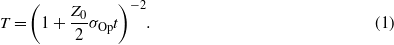
Here, Z0 is the impedance of free space (377 Ω) and σOp is the optical conductivity, which like T is a function of wavelength, λ [9]. (We note that expansion of equation (1) shows it to be identical to the Lambert–Beer law, T = e−αt, to first order. This shows σOp to be related to the absorption coefficient, α, by σOp ≈ α/Z0.)
By combining equation (1) with the definition of sheet resistance (for a bulk-like film),

(σDC,B is the bulk DC conductivity of the film i.e. the conductivity of a film which is thick enough such that the DC conductivity is thickness independent) to eliminate t, one obtains a relationship between T and Rs [16]:
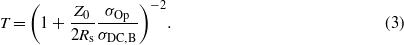
Here σDC,B/σOp can be considered a figure of merit, with high values giving the required properties (high T coupled with low Rs). However, while equation (3) tends to provide an excellent fit to (T,Rs) data for relatively thick networks of various nanoscale conductors, the agreement breaks down for thinner networks [23, 10, 46, 47]. As thin films are required to give high T, this can be a significant problem. Recently, we showed that equation (3) does not usually apply in the technologically relevant region around T = 90% [30]. This is because, for thin networks, the DC conductivity is no longer thickness independent but follows a percolation-like thickness dependence [48]: σDC ∝ (t−tc)n, where t is the estimated thickness of the network, tc is the critical thickness, i.e. the percolation threshold, and n is the percolation exponent. Approximating t − tc ≈ t, this leads to a new relationship between T and Rs which applies to thin networks [30]:
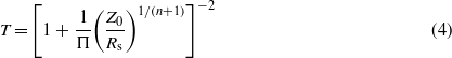
where we denote Π as the percolative figure of merit (FoM),
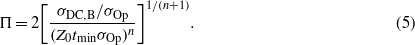
Here, tmin is the thickness below which the DC conductivity becomes thickness dependent (i.e. equation (4) applies for thicknesses below tmin). Analysis of these equations shows that large values of Π, but low values of n, are required to achieve low Rs coupled with high T [30].
Inspection of equations (3)–(5) shows that the optical and electrical properties of nanowire networks are completely described by the parameters σDC,B/σOp, tminσOp and n. Thus, in order to understand the dependence of network properties on wire dimensions, it will be necessary to measure the dependence of these properties (and the composite property, Π) on nanowire length and diameter.
2. Experimental procedure
Silver nanowires were synthesized by Seashell Technologies (www.seashelltech.com/) and supplied as suspensions in isopropyl alcohol (C = 12.5 mg ml−1 as measured by thermogravimetric analysis). A small volume of the dispersion was diluted to 0.001 mg ml−1 with Millipore water. In general, this was subjected to 5–20 min low power sonication in a sonic bath (Model Ney Ultrasonic).
Silver nanowire films were prepared by vacuum filtration of the above dispersions using porous mixed cellulose ester filter membranes (MF-Millipore membrane, mixed cellulose esters, hydrophilic, 0.22 µm, 47 mm). The deposited films were dried on a hotplate (50 °C) followed by a wet transfer to a polyethylene terephthalate (PET) substrate using heat and pressure [20]. The cellulose filter membrane was then removed by treatment with acetone vapour and subsequent acetone liquid baths followed by a methanol bath [20]. The film was 36 mm in diameter.
Scanning electron microscopy measurements were made using a Zeiss Ultra scanning electron microscope. Charging was avoided by transferring the AgNW film from the cellulose membrane to a silicon substrate coated with a thin gold film. Optical transmission spectra were recorded using a Cary Varian 6000i, with a sheet of PET used as the reference. Sheet resistance measurements were made using the four probe technique with silver electrodes of dimensions and spacings typically of the order of millimetres in size and a Keithley 2400 source meter.
3. Results and discussion
3.1. Scanning electron microscopy of wires and films
In order to understand the effect of nanowire dimensions on the optical and electrical properties of nanowire networks we acquired a number of batches of silver nanowires from Seashell Technologies. These had mean diameters, D, between 61 and 127 nm and mean lengths between 3.4 and 8.7 µm (see SI for histograms (available at stacks.iop.org/Nano/23/185201/mmedia), figures 1(A) and (B) for images and table 1 for data). These wires were provided as dispersions in isopropanol and could easily be formed into networks by vacuum filtration on to porous membranes [23]. These networks could then be transferred onto PET or glass substrates by standard methods [20]. Depending on the combination of dispersion volume and nanowire concentration, the deposited nanowire mass can be controlled, resulting in the control of network thickness. Examples of both sparse and thick networks are shown in figures 1(C) and (D) respectively. Once these networks have been deposited, it is straightforward to characterize their electrical and optical properties.

Figure 1. SEM images of (A) low diameter silver nanowires (D = 61 nm), (B) large diameter silver nanowires (D = 127 nm), (C) a sparse network and (D) a thick network.
Download figure:
Standard imageTable 1. Measured parameters for each wire type. Note that the values of σDC,B/σOp and Π given in this table are as-measured and not rescaled to represent the case when L = 5 µm.
| D (nm) | L (µm) | σDC,B/σOp | Tx (%) | Π | n |
|---|---|---|---|---|---|
| 61 | 4.0 | 140 | 37 | 42 | 0.59 |
| 64 | 3.4 | 151 | 67 | 56 | 0.67 |
| 88 | 4.4 | 153 | 61 | 20 | 1.53 |
| 127 | 8.7 | 205 | 83 | 30 | 2.44 |
3.2. Dependence of electrical properties on nanowire length
In order to understand the dependence of electrical and optical properties on both D and L, it will be necessary to treat these parameters separately. To do this, we take nanowires with a particular mean diameter (D = 84 nm) and use sonic energy to cut them up to give a number of sets of wires, each with the same mean diameter but with different mean lengths. Specifically, a dispersion of nanowires with initial length of 6 µm was sonicated in a sonic bath for a period of 60 min. At various times aliquots were removed. The wires were deposited on a substrate and the length measured by SEM. Shown in figure 2(A) is the measured mean nanowire length as a function of sonication time, τ. It is clear from these data that the length follows a power law: L ∝ τ−0.34. This exponent is reasonably close to the value of − 0.5 expected assuming that sonication induced scission is responsible for the cutting process [49, 50]. In addition, for each sonication time both a thick film (2–3 µm) and a thin film (200–300 nm) was prepared by vacuum filtration. The thicknesses of these films were estimated by breaking the films and imaging the cross section by SEM. We note that this method, like all methods of thickness measurement for nanostructured thin films, is somewhat unreliable. However, in this experiment the variation in conductivity over the range of nanowire lengths was large enough that the thickness-related error in conductivity was acceptable. For the thick films, the sheet resistance was measured and σDC,B calculated using equation (2). As all films were many times thicker than the nanowire diameter, they are expected to display bulk-like electrical properties [30]. Figure 2(B) shows that σDC,B increases monotonically as a function of L. We attribute the scatter to the difficulties in measuring the film thickness. Hecht has argued that the conductivity should scale with nanowire length as a power law: σDC,B ∝ Lα with exponent in the range 0 ≤ α ≤ 2.48 [51]. Indeed by studying networks of carbon nanotubes, Hecht found α = 1.46. It is clear from figure 2(B) that a power law is appropriate for our data but with exponent α = 0.9 ± 0.2. In fact this result is consistent with a linear relationship as shown in the inset of figure 2(B). For the rest of this paper we will assume a linear relationship: σDC,B ∝ L. For the thin films, we measured the optical transmittance (550 nm) and used the estimated thickness to calculate σOp using equation (1). These data are shown in figure 2(C) and strongly suggests the optical conductivity to be independent of nanowire length.
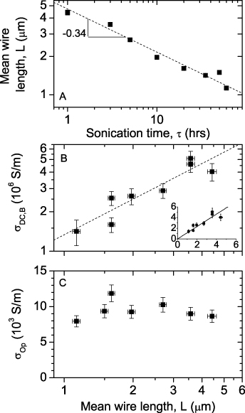
Figure 2. (A) Mean wire length as a function of sonication time. (B) Bulk DC conductivity of thick films (t ∼ 2–3 µm) as a function of mean nanowire length. The dashed line represents the best power law fit. Inset: linear scale. The solid line described the best linear fit: σDC,B = 1.16 × 10¹²L. (C) Optical conductivity, measured for thin films (t ∼ 200–300 m) as a function of nanowire length.
Download figure:
Standard image3.3. Measurements of T and Rs for networks of wires with different dimensions
Once the effect of L is understood, it is necessary to investigate the effect of D on the optoelectrical properties of nanowire networks. In order to ascertain the diameter dependence, we prepared four sets of networks, corresponding to the four wire types (61 nm ≤ D ≤ 127 nm, table 1). Each set consisted of networks with a range of different thicknesses. Although it is difficult to accurately measure the network thickness, we estimate the mean thicknesses to vary from ∼10 nm to ∼8 µm. (We note that the thinnest networks have mean thickness lower than the mean wire diameters. This mean thickness is defined as the thickness of a continuous film with density equal to that of the network. Because the networks are very porous, these mean thicknesses can be much lower than the wire diameter.) In each case we measured the sheet resistance and transmittance (550 nm). The transmittance spectra are shown in figure 3 and are typical of AgNW networks. The transmittance at 550 nm is plotted as a function of Rs in figure 4. In all cases we see an increase in transmittance coupled with an increase in sheet resistance as the network thickness decreases. These data sets can now be analysed using a number of models.
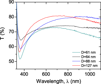
Figure 3. Transmittance spectra of networks of nanowires with four different diameters.
Download figure:
Standard imageAs described in section 1, it is thought that nanostructured networks only display thickness independent (i.e. bulk-like) DC conductivities for thickness above some critical value, tmin. In contrast, thinner films are controlled by percolation and have DC conductivity which varies with thickness. As a result, we can fit the thicker (i.e. low T and low Rs) films with bulk-like theory as described by equation (3) (see dashed lines in figure 4) and the thinner (i.e. high T and high Rs) films with percolation theory as described by equation (4) (see solid lines). In all cases good fits are obtained. From these fits, we can get σDC,B/σOp, Π and n (table 1). Indirectly, we can also find tminσOp. These parameters will be described in subsequent sections.

Figure 4. Transmittance-sheet resistance curves for the four nanowire types used in this study. In each case, the data can be divided into two regimes, the bulk-like regime and the percolative regime. These regimes have been fitted using equation (3) (dashed line) and equation (4) (solid line) respectively. Illustrated in figure 3(A) is the meaning of the quantity Tx discussed in the text.
Download figure:
Standard image3.4. Dependence of bulk parameters on nanowire diameter
From the fits of equation (3) to the data in figure 4, we can obtain σDC,B/σOp for each nanowire diameter, finding values between 140 and 205 as reported in table 1. These values are in line with those found recently by analysing [47] literature data for networks of metallic nanowires using equation (4), giving values of σDC,B/σOp between 83 and 453 [31, 34]. However, our values cannot be compared directly with each other, as they are for nanowires with different lengths. To make them comparable we use the knowledge that σDC,B ∝ L to rescale the data to represent wires with the same length i.e. L = 5 µm (we note that σOp is invariant with L). The rescaled σDC,B/σOp data are shown as a function of D in figure 5. These data can be fit well to a power law σDC,B/σOp ∝ D−β with β = 0.8 ± 0.2 (see figure caption for equation of fit curve). This rather low value of β implies that the optoelectrical properties of nanowire networks vary rather slowly with D. We had predicted [30] this exponent to be considerably larger (i.e. β = 3) based on theoretical estimates that σDC,B ∝ D−3 [52]. That this is not the case suggests that either the predicted D dependence of σDC,B is wrong or that σOp also scales with D. Combining this measurement of β with the length dependence discussed previously allows us to approximately write σDC,B/σOp ∝ L/D.
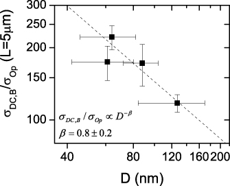
Figure 5. The conductivity ratio, σDC,B/σOp, extracted from the bulk fits in figure 2 plotted as a function of mean nanowire diameter. Because the mean wire lengths are different for all samples, the data has been rescaled to represent the ratios expected for sample of wires with the same mean length of 5 µm. This rescaling was based on the linear relationship between σDC,B and L observed in figure 2(B). The dashed line is a power law fit to the data; σDC,B/σOp = 4.27 × 10⁻⁴D−0.79 (D in metres).
Download figure:
Standard imageIdeally, it would be of interest to measure the diameter dependence of σDC,B and σOp independently. The most obvious way to do this is to measure the film thickness and use the T and Rs data coupled with equations (1) and (2) to find σDC,B and σOp for each wire type. However, as indicated above, it is difficult to accurately measure the thickness of such networks. In particular the small range of wire diameters available means that variation of σDC,B and σOp with diameter is not likely to be enough to overcome the thickness-related errors. In fact during this work we found that the errors associated with our film thickness measurements were so large as to make any comparative analysis of σDC,B and σOp completely unreliable. Thus, we found it impossible to accurately measure the diameter dependence of σDC,B and σOp.
However, it is worth noting that, as described above, we do not need to know σDC,B and σOp individually. In fact, once σDC,B/σOp is known, the system can be fully described so long as tminσOp and n are known. As we will see, n can be found from fitting the data with equation (4). This means we need to find a way to estimate find tminσOp. We can do this by noting that where both bulk-like and percolative behaviour are observed, it is possible to obtain information from the measured transmittance (Tx) where the transition from bulk-like to percolative occurs (see figure 4(A) for an explanation of this parameter). Noting that the film thickness when this transition occurs is tmin, we can rewrite equation (1) in this special case as

As Tx can be read directly from figure 4 (see table 1) it is straightforward to obtain σOptmin for each wire type. These data are shown in figure 6 as a function of wire diameter. It is clear from these data that σOptmin scales with D as a power law with exponent 1.8 ± 0.6 (see figure caption for equation of fit curve).
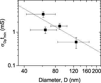
Figure 6. Proxy for optical conductivity as a function of mean nanowire diameter. The dashed line is a power law fit to the data; σOptmin = 3.98 × 10⁻¹⁶D−1.77 (SI units).
Download figure:
Standard image3.5. Dependence of percolation parameters on nanowire diameter
The low thickness (high T and high Rs) portions of the curves in figure 4 were fitted using percolation theory as described by equation (4). From these fits, one obtains the percolation exponent, n, and the percolative figure of merit, Π, for each wire type. These data are plotted as a function of wire diameter in figure 7. Figure 7(A) shows that the percolation exponent increases with increasing diameter from ∼0.6 to ∼3.5. We note that lower values of n lead to lower Rs, coupled with higher T. Again this suggests that low D wires are desirable. Empirically this appears to be very close to a quadratic dependence (see figure caption for fit equation). It is well known that the percolation exponent can deviate from its universal value of 2 in the presence of a distribution of inter-wire junction resistances with the magnitude of the deviation scaling with the details of the distribution [53–56]. It is likely that a disordered network will have a broad distribution of junction resistances and so larger n. Indeed, such a relationship has recently been observed for spray cast AgNW networks where n was observed to scale linearly with the network non-uniformity [36]. In light of this, our data suggests that the network non-uniformity tends to increase with increasing wire diameter. This clearly suggests that for networks in the percolative regime, low diameters are advantageous because low values of n lead to better optoelectrical properties but also because they lead to more uniform networks.
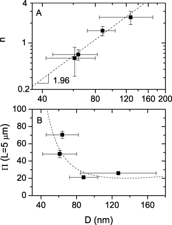
Figure 7. Percolation fit constants as a function of mean wire diameter, D. (A) The percolation exponent, n, and (B) the percolative figure of merit, Π. In (A) the data has been fitted to an empirical power law; n = 9.12 × 10¹³D1.96 (D in metres) In (B) the data has been rescaled to represent the values expected for samples of wires with the same mean length of 5 µm (this was done by multiplying the original values of Π by (5 µm/L)1/(n+1)). The dashed line in (B) represents a continuous function calculated using equation (5) incorporating the empirical fit curves shown in figures 5, 6 and 7(A).
Download figure:
Standard imageThe percolation fits also give values for Π as shown in table 1. However, as with other data these values must be corrected for the varying length. We rescaled the data to represent the values expected for samples of wires with the same mean length of 5 µm (this was done by multiplying the original values of Π by (5 µm/L)1/(n+1)). The rescaled data are shown in figure 7(B) as a function of D. Here Π increases sharply as D decreases, reaching ∼70 for D ∼ 60 nm. That higher values of Π lead to lower Rs, coupled with higher T, again suggests that low D wires give better optoelectrical properties. We note that values of Π approaching 70 are extremely high. Recently, we analysed literature data for networks of metallic nanowires using equation (4). The highest value of Π we found was 48 for networks of copper nanowires [47].
As described above, Π is a composite parameter defined by equation (5). The more fundamental parameters controlling Π are σDC,B/σOp and tminσOp and n. However, for each of these parameters we have generated empirical expressions by fitting the data in figures 5, 6(B) and 8(A) (see captions for equations). These expressions can be substituted into equation (5) to give a semi-empirical expression for Π as a function of D. This is shown in figure 7(B) as the dashed line and clearly shows the rapid increase in Π for D < 80 nm.
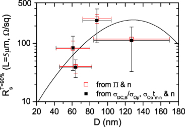
Figure 8. The estimated sheet resistance associated with a film of transmittance of 90%,  , plotted as a function of mean wire diameter. The data points represent
  calculated two ways: using values of Π and n found for each wire type using equation (7) and using values of σDC,B/σOp, σOptmin and n using equation (8) (in each case the values used were those rescaled to represent samples of 5 µm long nanowires). The solid line represents a continuous function calculated using equation (8) incorporating the empirical fit curves shown in figures 5, 6 and 7(A).
Download figure:
Standard image3.6. Resistance for 90% transparency
The data described above show that lower values of D give better values of n and Π, with respect to optoelectrical applications. However, having two parameters describing the performance is not ideal. A single FoM which could directly be linked to performance would be much more desirable. We note that for industrial applications the transmittance generally needs to be above 90% while the sheet resistance must be as low as possible. With this in mind, a useful parameter is the sheet resistance of a film with T = 90%,  . As networks with T = 90% generally reside in the percolative regime [47], this can be found by rearranging equation (4):

(here the factor of 0.054 comes from setting T = 90% in the factor (T−1/2 − 1)). Alternatively, we can write  in terms of more fundamental quantities by combining equations (4) and (5) and reorganizing the resultant expression to give

(here the factor of 0.11 comes from setting T = 90% in the factor 2(T−1/2 − 1)). This expression displays an exponential relationship between  and n, underlining the importance of n and so network uniformity. We have used both these expressions to calculate
  using the data described above for each wire type (figure 8). Although there is some scatter and considerable uncertainty, these data clearly show that lower diameter wires give better values of
  . To make the diameter dependence clearer, we have used the empirical expressions for σDC,B/σOp and tminσOp and n described above to generate a semi-empirical expression for
  as a function of D. This is shown as the solid line in figure 8. These data clearly show that very low values of
  can be expected if wires with very low D can be produced. The curve also decreases at high D due to the reduction in σOp with increasing D. However, networks of wires with such high D would exhibit significant haze [31] and be extremely non-uniform and so be unsuited to practical applications. We note that the analysis described above does not include the fact that the conductivity of metallic nanowires begins to fall as D is reduced below 50 nm [57]. Measurements have shown the nanowire conductivity to fall by a factor of 2 as D is reduced from 50 to 25 nm [57, 58]. Incorporating this effect means that the actual value of
  may be up to a factor of 2 higher than that predicted in figure 8 depending on the balance of nanowire and junction resistances. While figure 8 predicts a value of
  for D = 25 nm, this means the true value at this diameter may be as high as
  . However, we note that we have not optimized the inter-nanowire junction resistance in this work. It can easily be shown that
  scales linearly with the junction resistance [59]. Thus, improvements in processing which result in a reduction in junction resistance will reduce these values even further. We suggest that the exceptionally low value of
  reported recently [39] stems from a combination of low D and low junction resistance. Thus moving to low diameter nanowires would give considerable performance enhancement. In addition, networks of AgNWs are usually strongly affected by haze due to light scattering by the wires. This effect should be significantly reduced by moving to lower D nanowires. In addition, the network would be considerably more uniform leading to more reliable performance, especially for small pixel applications.
4. Conclusion
We have measured the transmittance and sheet resistance for a large number of networks of silver nanowires with different lengths and diameters. We find that, while the bulk-like DC conductivity of the networks scales linearly with wire length, the optical conductivity is invariant with wire length. The ratio of DC to optical conductivity, often used as a figure of merit, scaled with wire diameter and length approximately as σDC,B/σOp ∝ L/D. We found that, in all cases, networks within the technologically relevant regime of T > 90% were described by percolation theory. In this case, the dependence of T on Rs is controlled by two parameters, the percolation exponent, n, and the percolative figure of merit, Π. We found n to decrease with decreasing D while Π increased with decreasing D. In both cases, this behaviour points to better optoelectrical performance for networks of lower diameter wires. We could check this by calculating the expected sheet resistance for a network with T = 90%. We found this quantity to fall rapidly with decreasing D. We estimate that, by preparing networks of wires with D = 25 nm, values as low as  could be obtained.
Acknowledgments
We acknowledge the Science Foundation Ireland funded collaboration (SFI grant 03/CE3/M406s1) between Trinity College Dublin and Hewlett Packard, which has allowed this work to take place. JNC is also supported by an SFI PI award.